New Batch Starts In a Week
Custom and analog layout 6 months course focused on all the aspects starting from Digital design, basics of semiconductors, fabrication, Linux, TCL scripting, Layout fundamentals, and detailed understanding of Analog, standard cell, memory and IO layout including physical verification.
Next Batch
1-1 Dedicated Mentor Support
24/7 Tool Access
Multiple Mock Interviews
Industry Standard Projects
Support with Resume Update
Custom and Analog Layout Training Overview
Course Overview
Custom Layout Training with multiple projects at 18nm tech node – Summary
Duration: 8 months comprehensive program
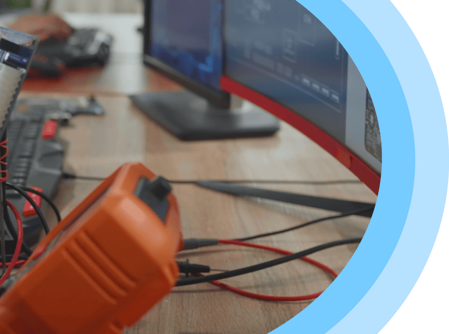
Tools:Synopsys Custom designer and Cadence Virtuoso tools (24×7 Tool access)
Placement Support: Institute provides placement support till candidate gets a Job
Training Highlights:
Analog Layout, Memory Layout, Standard Cell and IO Layout Design
CMOS, FinFET technologies and various memory architectures
Detailed understanding of VLSI Design Flow and Advanced Digital Design
Linux commands, scripting, version control, and soft skills for interviews
Core Electronics Foundation:
Semiconductors, Ohm’s Law, Kirchhoff’s Laws
Diode and MOSFET operation with second-order effects
FinFET technology and complete IC fabrication process
Layout Techniques:
Standard Cell Layout Design
Memory Layout and IO Layout for multiple architectures
Analog Layout Techniques including Matching and Noise Mitigation
Analysis of Electro Migration, IR Drop, Antenna Effect, WPE, LOD, Latch-up, and ESD issues
Hands-on Training:
20+ lab sessions and detailed assignments across all layout areas
Real-time projects in Standard Cell, IO, Memory, and Analog Layout
Analog Layout Projects:
Common Centroid and Interdigitation Techniques
Resistor and Capacitor Matching
Opamp Layout, Current Mirrors, PLLs, ADCs, DACs
Bandgap References, Temperature Sensors
Current and Voltage Bias Lines, Large Drivers, LNAs, Mixers
Sense Amplifier and Bit Cell Development
Training Delivery:
Comprehensive theory + lab sessions guided by industry experts
Practical exposure using real-time design examples
Program Highlights:
End-to-end Custom Layout expertise from basics to advanced analog design
Emphasis on failure mechanisms and robust layout strategies
Industry-standard practices and tools throughout the course
Institute Info:
Offered by VLSIGuru, established in 2012
Trained over 10,000+ students
Affordable in-class training in Bangalore
Online training available for students outside Bangalore
Detailed overview:
Custom Layout Training is a 8-month course done using both Synopsys custom compiler and Cadence Virtuoso tools. it provides deep technical expertise in all major layout domains including Analog, Memory, Standard Cell, and IO layout.
The course prepares students in both theoretical and hands-on aspects of VLSI physical design, including advanced CMOS and FinFET layouts, failure mechanisms, fabrication processes, and analog layout techniques. Extensive hands-on labs and projects build the necessary skills to succeed in layout design roles in the VLSI industry.
Custom layout training is a 8 months course focused on all the aspects of layout including Analog layout, Memory layout, Standard cell layout and IO layout.
Custom layout design course ensures that the student is prepared on all the essential aspects of Custom layout including VLSI Design flow, advanced digital design, CMOS, FinFET, various memory architectures, Standard cell, IO’s and detailed analog layout techniques. Course also includes training on Linux commands, version control, scripting and soft skill for effective interview performance.
Course also includes detailed sessions on semiconductors, Ohms law, Kirchoff law’s, Diode-operation, MOSFET’s, MOSEFT operations, second order effects, FinFET’s, and detailed fabrication process, which is followed by assignments and hands on projects.
Course also covers layout basics, hands on standard cell layouts, IO layout and memory layout for different architectures. Followed by various analog layout techniques with detailed discussion on Mismatches & Matching, Noises & Coupling, various failure mechanisms which includes Electro migration, IR drop, LOD & Stress effects, WPE, Antenna Effects, Latch up, ESD. Course includes 20+ detailed labs & assignments covering all aspects of custom layout with multiple hands on projects.
Analog layout techniques involve multiple hands on projects covering various concepts such as common centroid, inter digitation, resistor matching, capacitor matching and opamp circuits, current mirrors, PLL’s, ADC’s, DAC’s, Bandgap, Temperature sensors & Biases -> Current & Voltage bias lines, Large drivers, LNA & Mixers, and Sense amplifier & Bit cell development.
Synopsys custom designer and Cadence Virtuoso
ASIC Flow Overview
- Requirements
- Design specification & architecture
- RTL Coding
- RTL integration
- Functional verification
- Synthesis
- DFT
- Physical Design
- STA
- Custom Layout
- Physical Verification
- Post Silicon Validation
Digital Design - Deep dive
- Combinational logic
- Number systems
- Radix conversions
- K-maps, min-terms, max terms
- Logic gates
- Realization of logic gates using mux's and universal gates
- Compliments (1/2/9/10's complement)
- Arithmetic operations using compliments
- Boolean expression minimization, Dmorgan theorems
- POS and SOP
- Conversion and realization
- Adders
- Half adder
- Full adder
- Subtractor
- Half subtractor
- Full subtractor
- Multiplexers
- Realizing bigger Mux's using smaller Mux's
- Implementing Adders and subtractors using Multiplexers
- Decoders and Encoders
- Implementing Decoders and Encoders using Mux and Demux
- Bigger Decoder/Encoder using smaller Decoder/Encoder
- Comparators
- Implementing multi bit Comparators using 1-bit Comparator
- Sequential logic
- Latch, Flipflop
- Latch, Flipflop using Gates or Mux's
- Different types of FFs
- FF Truth table
- Excitation tables
- Realization of FF's using other FF's
- Applications of FF's, Latches
- Counters
- Shift registers
- Synchronizers for clock domain crossing
- FSM's
- Mealy, Moore FSM
- Different encoding styles
- Frequency dividers
- Frequency multiplication
- STA
- Setup time, Hold time, timing closure
- fixing setup time and hold time violations
- Launch flop, capture flop
Linux commands – hands on training
- Unix Operating System
- Kernel
- Unix Shells, RC files
- Shell scripting basics (as required for job)
- Unix Directory structure, hard/soft links
- Xterm, Xhost, commonly used commands
- Text editors
- Revision Management
- Makefile, Cronjob
- Mapping Unix directories, file with Gvim editor
- FTP, SCP, Mail, Compress, sleep, regular expressions
- LSF, Batch submission, Process monitoring
- Revision Management with hands on labs
Electronic circuits
- Basic Passive and Active devices.
- Ohms law, Kirchoff laws
- Basic of circuit understanding
CMOS & FINFET Basics
- Transistors in hardware design
- Significance of transistors in hardware design
- Logic gate implementation using BJT, CMOS
- MOSFET functionality
- Semiconductors
- What makes Semiconductor special element?
- Classification of solids into three types
- Conductor, Insulator, Semiconductor
- Energy bands in Solids
- Types of Semiconductors
- Intrinsic Semiconductors
- Extrinsic Semiconductors
- Types of Extrinsic Semiconductors
- N-type Extrinsic Semiconductor
- P-type Extrinsic Semiconductor
- Si, Ge – comparison
- Types of current in Semiconductors – Drift, Diffusion
- Ion
- PN Junction diode
- PN Junction – forward, reverse bias
- V-I Characteristics of PN Junction Diode
- Different types of Diode
- Applications of Diode
- BJT
- BJT
- BJT working principle?
- How BJT can be used for large scale manufacturing
- BJT fabrication steps
- Types of BJT?
- Why BJT is not used in for lower technology nodes?
- Issues with BJT?
- Advantages of BJT?
- NAND gate using BJT?
- Field Effect Transistor : FET
- What is Field Effect Transistor?
- Types of FET
- NMOS
- PMOS
- CMOS
- Fin
- NMOS
- NMOS
- What is NMOS?
- NMOS working principle?
- Different voltages, currents, their equations
- NMOS circuit representation
- How NMOS works like a switch
- How NMOS can be used for large scale manufacturing
- NMOS fabrication steps
- Types of NMOS?
- Why CMOS is used instead of NMOS?
- Issues with NMOS?
- Advantages of NMOS?
- NAND gate using NMOS?
- CMOS
- CMOS
- What is CMOS?
- CMOS working principle?
- Different voltages, currents, their equations
- CMOS circuit representation
- How CMOS works like a switch
- How CMOS can be used for large scale manufacturing
- CMOS fabrication steps
- Types of CMOS?
- Issues with CMOS?
- Advantages of CMOS?
- NAND gate using CMOS?
- CMOS second order effects?
- FinFET
- FinFET
- What is FinFET?
- FinFET working principle?
- Different voltages, currents, their equations
- CMOS circuit representation
- How CMOS works like a switch
- How FinFET can be used for large scale manufacturing
- FinFET fabrication steps
- Types of FinFET?
- Issues with FinFET?
- Advantages of FinFET?
- NAND gate using FinFET?
IC fabrication
- Layers of CMOS
- Depositing oxide layer
- Photolithography
- Masking
- Etching Layers
- Formation of nwell
- Self aligned gate fabrication process
- Diffusion to create n+ and P+ regions
- Metallization
TCL scripting
- Overview
- Env Setup
- Special Variables
- Data Types
- Variables
- Operators
- Decisions
- Loops
- Arrays, Strings, Lists, Dictionary
- History and Redoing of commands
- String Pattern Matching commands
EDA tools used in the training
- Custom Compiler
- Schematic drawing
- Primewave simulator
- Transient analysis
- DC analysis
- AC analysis
- Noise analysis
- Custom Compiler
- Layout drawing
- IC Validator - Physical verification
- DRC
- Comparisons
- LVS
- NVN
- LVL
- StarRC
- LPE - Layout parasitic extraction
- Primewave simulator
- Post Layout simulation
- Redhawk
- Reliability analysis - theoretical aspects
Layout tool
- Layout Editor Tool
- Understanding the schematic symbols and parameters
- Creating and managing libraries and cell
- Commands for Layout editing.
- Commands for schematic editing.
- Verification : DRC and LVS
- Antenna effect, latchup, Electromigration, IR Drop
- Analog Layout of OpAmp, Current Mirror, PLL, ADC, and DAC
- Resistor, Capacitor layout techniques
- CMOS and BiCMOS layout techniques
- Standard Cell Layout : Inverter, AND, OR, NAND, NOR, AOI, OAI, Latches, and Flop
Pre layout simulation to Post layout simulations
- Schematic entry
- Early parasitics
- Estimated parasitic assistant
- Reliability analysis
- Static circuit checks(CCK)
- Pre-layout simulation and analysis
- Standard cells
- Analog circuits
- Analog and mixed mode circuits
- Layout
- Analog and Digital co-design
- Fusion compiler co-design
- IC Compiler II co-design
- IC Compiler co-design
- In-design error checks
- DRD
- IC Validator live DRC
- Via checks
- Metal Density analysis
- Color decomposition
- In-design electrical checks
- Electro migration
- Resistance
- Capacitance
- Shield coverage
- Voltage annotation for VDRC
- Early parasitics
- Estimated parasitic assistance
- Partial layout extraction
- Power device design
- Power device designing
- Analog design migration
- Schematic migration
- Layout migration
Advanced Layout Concepts
- Mismatches and Matching
- Techniques
- Interdigitation
- Common centroid
- Failure Mechanism
- Electro migration
- IR drop
- LOD & Stress effects
- WPE, Antenna Effects
- Latch up
- ESD
- High voltage rules
- EOS effects
- Noises & Coupling
- Different Types of process
- Advantages & Disadvantages of below
- Planar CMOS
- FD-SOI
- SOI
- Bi-CMOS
- Gallium Arsenide
- Silicon-Germanium
- Finfet
- Full Chip Construction
- Scribe Seal
- Pad Frame
- Integration and guidelines
- Packaging
Standard cell, IO, and Memory Layout
- Std Cell & Memories.
- IO Layout Guidelines : High speed IOs and High Speed Interfaces.
- Sense amplifier & Bit cell development
- Why memory layout different than analog layout
- Memory layout flow
- Types of memory layout (SRAM/DRAM/ROM)
- Introduction to SRAM memory layout
- Fixing few manually created leaf-cell errors which impact
- Abutment issues
- Impact of IR, EM and DFM .
- SRAM memory design architecture
- Words line and address line
- SRAM rows and column design
- Building blocks of SRAM
- Memory Bit cell
- Row decoder
- Word line driver
- Sense amplifier
- Control block
- Misc digital logic.
- Pitch Calculation for blocks.
- Power Planning
Analog and Mixed signal Layout
- High speed Analog Layout
- RF Layout guidelines with Transmission lines and inductor concepts
- Handling clocks
- Analog Circuits & Layout guidelines
- Single & Multi stage differential opamp layout
- current mirror layout
- PLL, DLL and Oscillators
- LDO and other regulators
- ADCs & DACs
- Bandgap, Temperature sensors & Biases -> Current & Voltage bias lines
- Large drivers
- input pair, differential routing, Power routing, offset minimising
- Power/Signal IR Drop
- cross-talk and coupling
- Electrostatic Discharge
- Deep Sub-micron Layout Issues
- Shallow Trench Isolation (LOD)
- Well Proximity Effect
Physical Verification concepts
- Design Rule Checks
- Layout Versus Schematic (LVS)
- Electrical Rule Checks (ERC)
- Antenna Checks
- Latch-up
- Reliability checks like EM and IR analysis
- Design for manufacturability (DFM)checks
- Electrostatic discharge (ESD) path checks
Assignments and hands on projects
- Assignments and multiple hands on projects
- Best Practices & Interview Questions.

Key Features
Who All Can Attend This Custom and Analog Layout Training?
This training is ideal for individuals aiming to build or enhance their expertise in analog/mixed-signal IC layout design, especially for low-power, high-performance semiconductor applications. It is suitable for both entry-level engineers and professionals in the VLSI domain.Pre-requisites To Take Custom and Analog Layout Training
- Expertise on Digital & Analog design concepts
- Exposure to basic layout concepts

High Demand for Custom and Analog Layout Training
Know about the Growing VLSI industry
Analog Layout Engineers are in high demand in analog/mixed-signal and RF design teams. Engineers with experience in deep sub-micron nodes (e.g., 28nm, 7nm) and knowledge of DRC/LVS, EMIR checks, and parasitic-aware layout get premium salaries. Major hiring hubs include Bangalore, Hyderabad, and Noida.
₹6.5 LPA
₹10 LPA
₹14 LPA
₹18 LPA
₹22+ LPA


- Customized training programs for teams
- Upskill and reskill employees with industry-relevant content
- Interactive sessions led by expert trainers
- Hands-on projects and real-world case studies
- Flexible delivery in online
- Improve productivity and efficiency
- Access to training resources and material

- Learn in real-time with instructor-led sessions
- Flexible access from anywhere
- Recorded sessions available for revision
- Training on industry-standard tools
- Get certification after completion

- Self-paced learning as per your flexibility
- Industry-aligned learning modules
- Certification after course completion
- Access to structured video lessons and materials
- Track your progress step by step
- Access to learning materials for more than 1.5 years
Custom and Analog Layout Training is crucial for developing deep expertise in critical VLSI domains like Analog, Memory, Standard Cell, and IO layout. This specialized training equips individuals with hands-on skills in advanced CMOS and FinFET technologies, analog layout techniques, and failure mechanism analysis, making them highly sought-after in the semiconductor industry for layout design roles.
Career Path
Learning Path


At VLSIGuru, we believe that education should lead to meaningful employment. Our training programs are designed not just to impart technical excellence, but also to bridge the gap between academic learning and industry demands. With a strong network of hiring partners and a proven track record, we ensure that our students are career-ready.
Placement Highlights
- Industry-aligned curriculum
- Hands-on projects and case studies
- Communication skills
- Resume building and interview preparation
- Technical and HR mock sessions
- Aptitude and domain-specific test series
- Regular drives and exclusive hiring events with partner companies
- Resume building and interview preparation

At VLSIGURU, we provide industry-focused VLSI training and guidance that helps students and professionals build strong technical skills and succeed in their careers. Our programs are designed to be practical, flexible, and aligned with current industry requirements.
Student Reviews


Frequently Asked Questions
- Expertise on Digital & Analog design concepts
- Exposure to basic layout concepts
- Course presentations for all topics
- Session notes
- Lab documents with detailed steps
- User guides
Our comprehensive Custom and Analog Layout Training program has a total duration of 6 months. This includes 2.5 months dedicated to basic concepts and 4 months focusing on advanced analog layout techniques and specialized topics.
Upon successful completion of all course modules, practical assessments, and the final project, you will receive a Certificate of Completion from VLSI Guru, validating your expertise in Custom and Analog Layout Design.
Yes, you can. We offer online training options specifically designed for students and professionals outside of Bangalore, providing the flexibility to learn at your own pace while managing your work schedule.
Our detailed syllabus includes a comprehensive overview of the ASIC flow, an in-depth exploration of digital design, Static Timing Analysis (STA), essential Linux commands, electronic circuit fundamentals, CMOS & FINFET basics, IC fabrication processes, TCL scripting, hands-on experience with industry-standard EDA tools, thorough training on layout tools, pre-layout to post-layout simulation techniques, advanced layout concepts including matching and failure mechanisms, standard cell, IO, and memory layout design, analog and mixed-signal layout techniques, and physical verification concepts.
Please contact our admissions team directly at [email protected] for detailed information on the course fee structure and any available discounts or payment options.
Our training is delivered through a combination of comprehensive theory sessions and extensive hands-on lab sessions, all guided by experienced industry experts. We emphasize practical learning using real-time design examples and provide 24/7 access to industry-standard EDA tools.
The issuance of a certificate is contingent upon the successful completion of all modules, assessments, and projects as outlined in our certification process. Incomplete training may not qualify for a certificate.
Our placement support involves actively assisting you in your job search. This includes helping you build a professional resume, preparing you for technical interviews, sharing job openings from our network of industry partners, and providing guidance until you successfully secure a job in the VLSI domain.
VLSI Guru graduates have been hired by numerous leading semiconductor companies and design services firms in India and globally. While we don't provide an exhaustive list, our alumni are working at prominent organizations in the VLSI ecosystem.
The starting salary for an Analog Layout Designer in India typically ranges from ₹4 LPA to ₹8 LPA. With increasing experience, specialized skills, and the company's size and location, experienced professionals can earn significantly higher salaries, often reaching ₹15 LPA or more.
Basic components of an analog layout include transistors (the core amplifying/switching elements), resistors (for setting current and voltage levels), capacitors (for filtering and energy storage), inductors (for filtering and RF circuits), and interconnects (metal layers for signal and power routing). Their purpose is to physically realize the designed analog circuit while meeting performance specifications, minimizing unwanted parasitics, and ensuring manufacturability and reliability.
Our course provides you with a strong foundation in both theoretical concepts and practical hands-on skills essential for analog layout design. The curriculum is industry-relevant, covering the latest technologies and tools. The placement support offered further enhances your job prospects by preparing you for interviews and connecting you with potential employers.
While our course provides a solid base, continuous learning is crucial. We encourage you to stay updated through industry publications, conferences, online forums, and by networking with professionals in the field. VLSI Guru may also offer advanced workshops or modules on emerging techniques in the future.
We provide comprehensive support throughout your learning journey, including guidance from experienced instructors, doubt clearing sessions, access to online resources and materials, 24/7 lab access, and placement assistance post-completion.
Yes, our training emphasizes extensive hands-on experience through 20+ detailed lab sessions and multiple real-time projects across various analog layout concepts, including Op Amps, current mirrors, PLLs, ADCs, DACs, and more. This practical exposure is a key highlight of our program.